
Page 2 - 湖北深紫科技有限公司----产品样册
P. 2
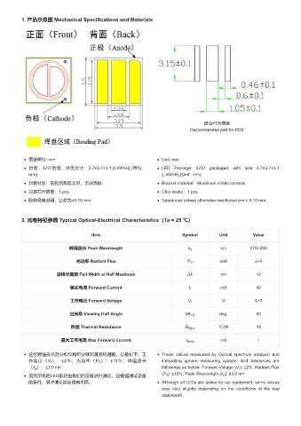
1. 产品示意图 Mechanical Specifications and Materials


                                                                                                                   建议PCB焊盘
                                                                                                           Recommended pad for PCB


                 图纸单位: mm                                                                   Unit: mm

                 封装:3737封装,外型尺寸:3.7×3.7×3.1 (L×W×H) [单位:                                    LED  Package:  3737  packaged,  with  size  3.7×3.7×3.1
                 mm]                                                                        (L×W×H) [Unit : mm]

                 封装材质:氮化铝陶瓷支架,半球透镜                                                          Bracket material:Aluminum nitride ceramic

                 封装芯片数量:1 pcs                                                               Chip inside:1 pcs

                 除非另有说明,公差为±0.10 mm                                                         Tolerances unless otherwise mentioned are ± 0.10 mm


             2. 光电特征参数 Typical Optical-Electrical Characteristics(Ta = 25 ℃)


                                                    Item                                               Symbol               Unit               Value


                                        峰值波长 Peak Wavelength                                              λ p               nm               270~280


                                            光功率 Radiant Flux                                              P 0               mW                  2~4


                                 波峰半高宽 Full Width at Half Maximum                                         Δλ                nm                  12


                                        驱动电流 Forward Current                                               I f              mA                  40


                                        工作电压 Forward Voltage                                              V f                V                  5~7


                                        出光角 Viewing Half Angle                                           2θ 1/2             deg.                60


                                         热阻 Thermal Resistance                                           R Θj-b            ℃/W                  18


                                   最大工作电流 Max Forward Current                                            I fmax             mA                   /


                 这些数值由光谱分析仪和积分球测量系统测量。公差如下:工                                                These  values  measured  by  Optical  spectrum  analyzer  and
                 作电压(V ):±2%;光功率(P ):±10%;峰值波长                                              integrating  sphere  measuring  system.  And  tolerances  are
                             f
                                                        0
                 (λ ):±3.0 nm                                                               followings as below: Forward Voltage (V ): ±2%, Radiant Flux
                                                                                                                                       f
                     p
                 虽然所有的LED都是由我们的设备进行测试,但根据测试设备                                               (P ): ±10%, Peak Wavelength (λ ): ±3.0 nm
                                                                                                                              p
                                                                                              0
                 的条件,某些值可能会略有不同。                                                            Although all LEDs are tested by our equipment, some values
                                                                                            may  vary  slightly  depending  on  the  conditions  of  the  test
                                                                                            equipment.